Simplified Communications – I²C and SPI
Many of today’s modern sensors, actuators, display, memory and other IC’s come with an external interface allowing them to be controlled from a master device. This master device could be a simple microcontroller or it could be something more advanced like a Linux based Raspberry Pi. By far the most commonly used interface buses used by these devices are I²C and SPI. Both I²C and SPI are available in Master and Slave modes with the Master controlling all operations and the Slave listening to what the Master is telling it.
Flowcode currently supports the Master versions of these buses with Slave functionality planned for the near future. Both I²C and SPI components in Flowcode have a Channel property which allows you to target a specific peripheral on-board your microcontroller or switch to software mode in which case the bus is bit-banged using standard I/O pins.
So what is I²C?
I²C (Inter-Integrated Circuit) is a bus originally developed by Phillips in 1982 which has subsequently been expanded and altered to create the I²C we know today. The bus consists of two signals SDA and SCL which stand for serial data and serial clock respectively. The bus can operate at various speeds which are generally dictated by the slowest device on the bus. Common bus speeds are 100K bits per second, 400K bits per second and 1M bits per second. The two bus signals can only be pulled low by the devices on the bus so they both require some kind of external pull up resistors. Sometimes the pull up resistor will be fitted into the slave device to reduce the number of external components. I²C is designed for fairly short range i.e. on the same PCB as the Master or via a relatively short cable. I²C devices may have external address pins which allows you to assign a unique address to each device and therefore allow multiple of the same device to operate on a single bus.
One of the great upsides of the I²C bus is that it can do voltage level shifting for you. For example say we have a Master running at 5V but a slave running at 3V3. The I²C pullup resistors are connected between the signals and 3V3 allowing the bus to float at 3V3. The Master can still recognise the 3V3 input voltage as a logic one and no nasty 5V is allowed to reach and potentially damage the slave.
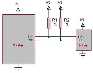
I²C Voltage Shifting Schematic
I²C has various operating states which generally always follow the same pattern, we have Start, Restart and Stop.
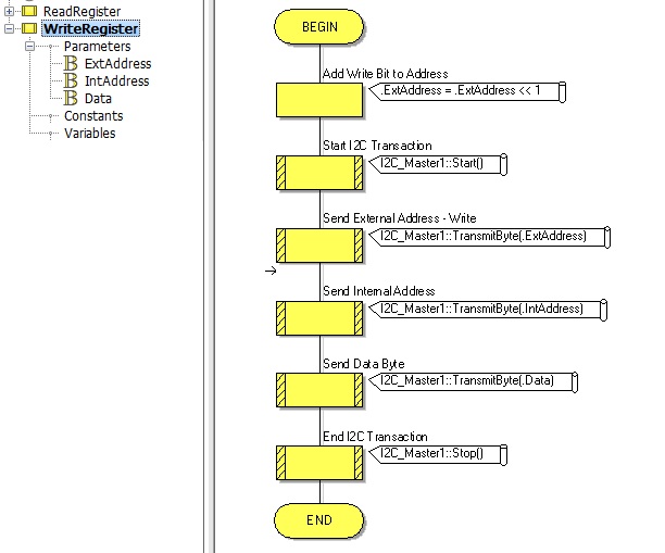
I²C Write Example
Here is an example to write a byte to a location on a typical I²C device. First we output a start condition to the I²C bus by using the start component macro. Next we transmit the device’s external 7-bit address specifying write mode. The address could be a simple fixed value or may combine a fixed value with external address pins for more flexibility. The read/write mode is signified by the least significant bit which is either a 0 for write or a 1 for read. The I²C device datasheet should detail the external address both with and without the read/write bit. In my examples I assume the address passed do not already contain the read/write bit. This explains the .ExtAddress << 1 which shifts the address up by one bit allowing room for the read/write bit.
Address Byte - AAAA AAAM
A = 7-bit Address
M = Mode of operation
Once the address byte has been sent we then transmit an internal address byte. Depending on how many registers the device has there might be more than one internal address byte to allow us to address each of the various registers or memory locations. Finally we send the data byte to write to the register location and finish with a I²C stop.
I²C Read Example
To read a data byte from a register requires a little bit more code as we have to startup in write mode to set the internal address and then restart into read mode to perform the read. Again we start by transmitting a send and using the 7-bit external address combined with the read/write bit in write mode. We then send the internal address like before. Next we differ from the write example by calling the restart component macro followed by re-sending the external address only this time with the read/write bit in read mode. We then use a receive byte component macro to receive the data from the internal register and complete the transaction with an I²C stop.
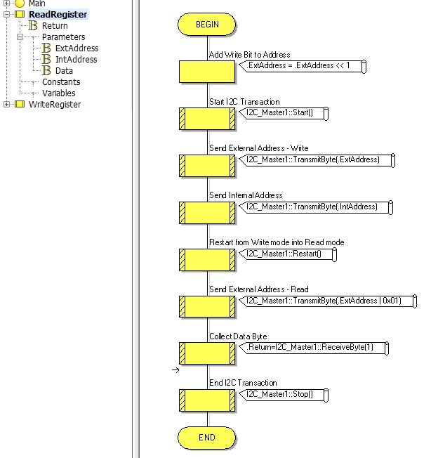
I²C can be a bit slow because of all of the setup to write or read a single byte. However there is a way of writing and reading multiple bytes by simply repeating the component macro Read/Write call before the I²C Stop is called. Each time you repeat the read or write the internal address will be automatically incremented. Note that the Read component macro has a parameter named Last, this should be set to 1 for the final read and 0 for all other reads which come before. This parameter just informs the slave device to expect more requests or not.
An example of I2C communications in practice can be found here: Quadrocopter 1 – MPU-6050 Accelerometer and Gyro
So what is SPI?
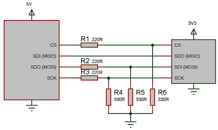
SPI (Serial Peripheral Interface) is a bus originally developed by Motorola. The bus consists of up to four signals SDO, SDI, SCK and CS which stand for serial data out, serial data in, serial clock and chip select respectively. There are other names for the data pins to better establish the master / slave connections, SDO is known as MOSI (Master Out Slave In) and SDI is known as MISO (Master In Slave Out). The bus can operate at various speeds which are generally dictated by the slowest device on the bus. Common bus speeds are in the 1-100M bits per second range. The bus signals can be pulled low and high by the devices on the bus so no external components are required apart from maybe a pull up resistor on the chip select (CS) pin to keep the bus disabled while the master boots up. SPI is designed for fairly short range i.e. on the same PCB as the Master or via a relatively short cable. Multiple SPI devices can be connected to the same SPI bus as long as they each have their own unique chip select (CS) pin connection from the master. Only one slave device on the bus can be active at any one time.
SPI is a lot less strict than I²C in that it does not have a rigid set of modes that need to be followed. The only real modes that SPI does have is active or disabled. There are however a set of configurations that can be done to the SPI bus namely what state the clock is in when idle and when in the clock cycle to sample to incoming data. One of the great advantages to the SPI bus is the high speed of operation allowing large quantities of data to be transferred quickly. Another advantage is that SPI is full duplex meaning it can receive data at the same time as transmitting data. In practice only one of the incoming or outgoing data bytes are generally put to use at any one time. 3-Wire SPI is a form of SPI used when one of the data signals is not required. For example a DAC device might not need the MISO signal and an ADC device might not need the MOSI signal.
SPI will not do voltage level shifting like I²C so care should be taken to check that the voltages are correct for both the master and slave. If possible it is recommended to run both the master and slave at the same voltage. However for something like a 5V master and 3V3 slave you can use potential dividers to reduce the voltage of the master’s output pins.
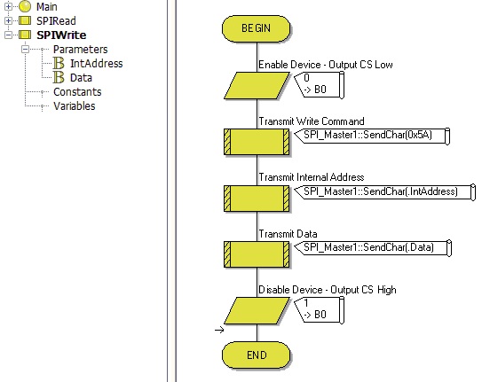
A typical SPI write operation might look like this.
Where as a SPI read operation might look like this.
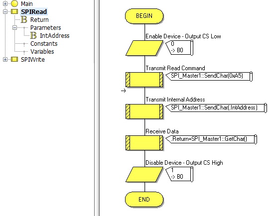
Again there may be additional address bytes or differing protocol for your device so refer to the device datasheet for the exact specifics. Note that the CS (Chip Select) signal is not provided as part of the SPI Master component and you have to manipulate it yourself either using an output icon in single bit mode or creating a single pin property and manipulating the output state using a calculation icon.
Pulling the chip select high has the effect of executing the operation on a lot of devices for example a DAC might not update it’s output voltage until a command has been clocked in and the chip select pulled high. You may also need delays after pulling the chip select high and pulling it low again for the next operation to allow time for the first operation to complete. Again this will be detailed in the device datasheet.
Conclusion
I²C and SPI buses are very simple to implement and open up a wide range of potential to your project. They are both designed for local use either on the same PCB as the master or via a short cable due to their high speed nature. Adding a interface header to your circuit board allow for future expansion and allows for things like process sharing. A good example of this would be a robot where there is a central brain that delegates fairly complex tasks like motor speed control to slave devices. This way the same host and multiples of the same slave can be used on a 2 wheeled robot and a 16 wheeled robot making the design very modular.
I²C is great for low speed or fairly infrequent communications whereas SPI can be used for much faster communications. Care must be taken when designing PCBs to avoid the high speed bus signals from going near sensitive signals such as low current analogue voltages as they may start to pick up some of the high frequency noise created by the bus.
Both buses essentially create a framework for operation however the actual protocol of bytes in and out will vary greatly from device to device. Flowcode provides the means of putting together the simple blocks which then allow you to create specific macros for specific devices. The examples show this type of mentality by creating parameter variables for things that can change and hard coding bits that will remain constant.
Both components will need their Initialise component macro calling before any other component macros from the component are called to put the bus into a ready state.
Both the I²C and SPI buses can be recorded in real time and decoded using the new Matrix Ghost Technology hardware and Flowcode 6 provided the buses are running at a low enough speed. This allows the communications and therefore the devices controlled by the comms to be easily debugged and analysed.
75,340 total views, 6 views today
Related Posts


About The Author
BenR
Embedded engineer with experience in Cybernetics (HMI), Robotics, Mechatronics, Control Systems and Communications using Microcontrollers and Microprocessors.
Nice and good to understand explanation of two ways of exchange data!
PLEASE if somebody has file flowcode+ isis PIC to PIC SPI Communication ;
Hi benchhida, get in touch with us via our website http://www.matrixtsl.com/contact.php and we will help you out as much as we can!
It is mentioned above:
“An example of I2C communications in practice can be found here: Quadrocopter 1 – MPU-6050 Accelerometer and Gyro”
I opened that link and downloaded the “quad1.zip” project and inside the project the communication seems with RS232 only and no I2C example.
Do I not see the I2C inside (hidden) or is it a mistake reference in the link above?
Looks like the file has changed to use a component instead of direct I2C calls. The MPU6050 component contains all the I2C calls.
If you click Build -> View C and then look at the SampleDevice funcion then you can see all the I2C macro calls.