Solar Energy Conversion
 This work introduces an approach to the design of a boost converter for a photovoltaic (PV) system using the MIAC. The converter is designed to step up the variable voltage provided by a solar panel to a stable 24V, without any batteries. The output of the boost converter is monitored by the MIAC and used to adjust the duty cycle of a PWM control signal of the boost converter.
Introduction
In recent years, attention towards renewable energy such as wind and solar power has increased dramatically. As more people are concerned with the power generation using fossil fuel which brings environmental problems, societies and conferences are being held to find solutions to slow down the world climate change caused by power generation.
Photovoltaic (PV) sources are used today in many applications from satellite power systems to battery chargers and home appliances. PV is an important green energy source because it has the advantages of being pollution free, low maintenance, with no noise or wear due to the absence of moving parts.
The power produced by a solar panel depends on two factors; irradiation and temperature. As irradiation and temperature levels change rapidly, the voltage produced fluctuates and becomes inconstant. A converter is therefore required to produce a constant voltage that is matched to the requirements of the load and supplied efficiently. A maximum power point tracker (MPPT) is a system that directs the converter to track the maximum power of a solar panel and deliver it to load (MPPT is not a mechanical tracking system that moves the solar panel to point more directly to the sun but it is an electronic system that varies the electrical operating point so that it will deliver a maximum output power). Within this context, this work presents the design of a converter using a high efficiency boost converter operating in continuous conduction mode (CCM). It is implemented with a control technique based on voltage feedback.
In this design, the proposed control algorithm will be simple compared to other MPPT control algorithms such as Perturbation and Observation (P&O) and Incremental Conductance (InCond). The voltage-feedback control algorithm is implemented using the MIAC which continuously tracks the output voltage of the boost converter and controls the duty cycle of the pulse-width-modulation (PWM) output signal used to drive the boost converter. As the PV output voltage changes, the duty cycle changes accordingly, allowing the converter to provide a constant output voltage.
As the converter produces constant output voltage, it can be coupled with another power conditioner unit and load. One application of this system is to supply power to a grid-tied inverter and produce an AC voltage that can send power into the utility grid as shown in Figure 1. In this application, the grid-tied inverter synchronizes and feeds power into the grid whereas the boost converter is used to condition the PV supply and provide the constant voltage required by the inverter. This grid connected system is characterized by the absence of storage elements, such as a battery. The main reason for the absence of storage elements is because of their size and high maintenance fees. Therefore, the whole system remains small and low cost. Furthermore, the converter unit can be attached to the solar panel as a single product. The proposed system could be easily implemented with analog circuits instead of a microcontroller, but the design above has the advantage of easy modification if additional renewable energy sources are used.
 Figure 1: Block diagram of proposed system for PV grid connected
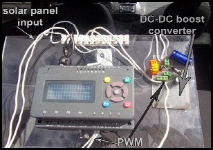
Figure 2: MIAC with DC/DC boost converter
Boost Converter Analysis
A simple boost converter consists of an inductor, a switch, a diode, and a capacitor as shown in Figure 2, the Boost converter circuit operation can be divided into two phases. Phase 1 begins when the switch SW is turned on at t = Ton as shown in Figure 3. The input current which rises flows through inductor L and switch SW. During this mode, energy is stored in the inductor. Phase 2 begins when the switch is turned off at t = Toff. The energy stored in the inductor causes its voltage to swap polarity and maintain current flow in the circuit, which is now directed through inductor L diode D, capacitor C, load R, and the supply of Vin as shown in Figure 2. The inductor current falls until the switch is turned on again in the next cycle. The reversing of the inductor voltage polarity in phase 2 allows the Vout to be greater than Vin
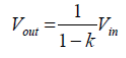
where Vout is the output voltage, k is duty cycle, and Vin is input voltage which in this case will be the solar panel voltage.

In order to operate the converter in continuous conduction mode (CCM), the inductance is calculated such that the inductor current IL flows continuously and never falls to zero as shown in Figure 3. Thus, L is given by :
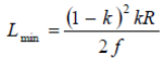
where Lmin is the minimum inductance, k is duty cycle, R is output resistance, and f is the switching frequency of switch SW.
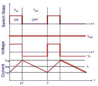
Figure 3: Output waveforms
The output capacitance to give the desired output voltage ripple is given by:

where Cmin is the minimum capacitance, k is duty cycle, R is output resistance, f is switching frequency of switch SW, and Vr is output voltage ripple factor. Vr can be expressed as:

Control Approach
A simple control technique is proposed in this paper. It uses voltage-feedback control technique where the output voltage of the boost converter is monitored continuously and compared with a reference voltage. The voltage difference is then used as a parameter in the control algorithm to allow the microcontroller to produce a PWM signal with the appropriate duty cycle. The PWM signal is then used to control the switch SW in the boost converter.
Figure 4. shows the flow chart of the voltage-feedback control technique whereas Figure 5. shows the monitoring process of the desired constant output voltage. With this control technique, any changes to the solar panel voltage will be compensated for in the converter to produce a constant output voltage.
 Figure 4: Control flow chart
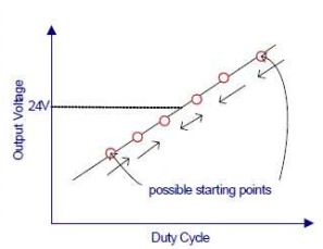 Figure 5: Output power monitoring process
Proposed System
As mentioned earlier, the proposed boost converter is implemented in between a solar panel and load as shown in Figure1. This system is able to deliver power with a constant output voltage of 24V without any storage elements such as a battery. Therefore, the converter remains small and light weight. In addition to that, the system is able to attach directly onto the solar panel to form a single unit.
Figure 1 shows that power stage including switch SW (which may consists of one or more parallel connected power MOSFETs), a fast switching type flyback diode D, an inductor L wound on ferrite core with an air gap to prevent core saturation, and an output capacitor C.
The controlling stage consists of a MIAC with a built-in analog-to-digital converter (ADC) and a PWM output. The control strategy based on the flow chart in Figure 4. is written and load into the MIAC. The MIAC uses the monitored voltage to perform calculations based on the control algorithm and produce a PWM output signal with the required duty cycle. The PWM signal is then transmitted to power the MOSFET in the power stage through a power MOSFET driver.
The MIAC unit features a 10-bit, successive approximation ADC, used by the control program to measure signals required for the power flow control; this is adequate for the proposed design. It also features two PWM outputs with program-controlled duty cycle and 469 kHz maximum frequency when driven by the 48 MHz clock of the unit. The first PWM output is used to control switch SW in the boost converter while the second PWM output can be used to control the switch in an auxiliary circuit such as zero voltage switching circuit and zero current switching circuit to reduce switching losses in boost converter.
The MIAC was chosen as the system controller because it has the necessary features for the proposed design such as built-in ADC, PWM outputs, eight-bit architecture, high clock rate, low power consumption and low cost. In order to calculate the value for Lmin and Cmin, the switching frequency will be set to the lowest value of 46.9 kHz. The rating of the proposed converter will be 130W and 24V output. By referring to (3), Lmin maximum will occur at k = 0.333 and the calculated value will be 1µH. As the desired output voltage ripple factor is below 1%, the calculated value of Cmin will be 687µF.. The converter switching frequency and the inductance value is compromised between the converter’s efficiency, cost, power capability and weight. For the control system, the MIAC will produce a PWM signal pulse train with varying duty cycle in the range of 0 to 1.0. Practically, the duty cycle for boost converter is only in the range of 0 to 0.75. This is due to the instability of the boost converter.

Easy setup wiring Complete system AC load

You can download our example program here, showing the necessary steps for adjusting the PWM output, alloowing for a constant output voltage.
6,396 total views, 4 views today


