Im using the custom component for ks108 lcd
Problem is im lost as i dont know which pin goes where, on the alphanumeric display you can select which port and pin each line goes to. with the custom component i cant do that.
When code is generated in C i just get this
//Common defines
#define MX_DATA_PORT portd //my value
#define MX_DATA_TRIS trisd //
#define MX_CONTROL_PORT portb //
#define MX_CONTROL_TRIS trisb //
#define MX_CS1 0 //
#define MX_CS2 1 //
#define MX_DAT_INST 2 //
#define MX_ENABLE 3 //
#define MX_READ_WRITE 4 //
This doesnt look right to me...
Is there something im missing, i want to be able to find the following
D0-D7 which pin is allocated the which, looking at the above code they appear to be on port D, but im not sure which pin on portD goes to Which pin on LCD
would it be like LCD- d0 --------Pic d0 and so on??
and i need to find the same for the control lines, i.e cs1, cs2, reset etc
I have looked at the readme file but the pinouts on there are different to my screen so there not 100% correct
Hope this makes sense, im only just learning so i might have confused you
Lcd Help, Pin allocation
-
cobra1
- Posts: 175
- Joined: Thu Feb 04, 2010 7:44 am
- Has thanked: 3 times
- Been thanked: 3 times
- Contact:
Re: Lcd Help, Pin allocation
This is my LCD pinout
Pin1...Vss
Pin2...Vdd
Pin3...V0
Pin4...RS
Pin5...R/W
Pin6...E
Pin7...DB0
Pin8...DB1
Pin9...DB2
Pin10..DB3
Pin11..DB4
Pin12..DB5
Pin13..DB6
Pin14..DB7
Pin15..CS1
Pin16..CS2
Pin17..Reset
Pin18..-10v
Pin19..LED+
Pin20..LED-
Pin1...Vss
Pin2...Vdd
Pin3...V0
Pin4...RS
Pin5...R/W
Pin6...E
Pin7...DB0
Pin8...DB1
Pin9...DB2
Pin10..DB3
Pin11..DB4
Pin12..DB5
Pin13..DB6
Pin14..DB7
Pin15..CS1
Pin16..CS2
Pin17..Reset
Pin18..-10v
Pin19..LED+
Pin20..LED-
-
Benj

- Matrix Staff
- Posts: 15312
- Joined: Mon Oct 16, 2006 10:48 am
- Location: Matrix TS Ltd
- Has thanked: 4803 times
- Been thanked: 4314 times
- Contact:
Re: Lcd Help, Pin allocation
Hello,
Here is an explaination of the component defines.
#define MX_DATA_PORT portd //my value
#define MX_DATA_TRIS trisd //
#define MX_CONTROL_PORT portb //
#define MX_CONTROL_TRIS trisb //
#define MX_CS1 0 //
#define MX_CS2 1 //
#define MX_DAT_INST 2 //
#define MX_ENABLE 3 //
#define MX_READ_WRITE 4 //
MX_DATA_PORT is the data bus pins:
Pin7...DB0 - RD0
Pin8...DB1 - RD1
Pin9...DB2 - RD2
Pin10..DB3 - RD3
Pin11..DB4 - RD4
Pin12..DB5 - RD5
Pin13..DB6 - RD6
Pin14..DB7 - RD7
MX_CONTROL_PORT is the remaining pins.
Pin4...RS - RB2
Pin5...R/W - RB4
Pin6...E - RB3
Pin15..CS1 - RB0
Pin16..CS2 - RB1
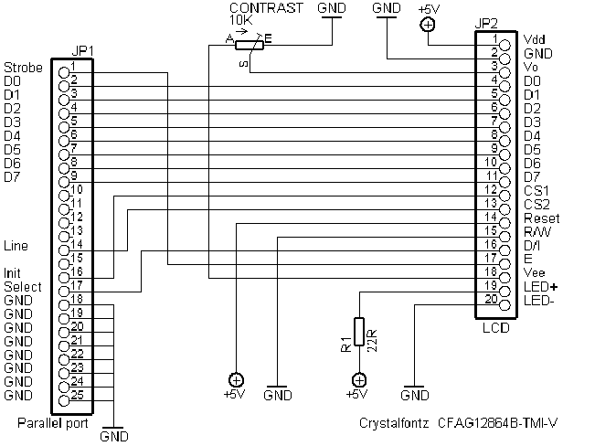
The other pins are not connected to the microcontroller and are controlled by your circuitry. There is a schematic here that shows how the other pins should be connected up for a working system. The reset pin should also be connected to the +5V.
http://www.skippari.net/lcd/sekalaista/ ... -TMI-V.png
Here is an explaination of the component defines.
#define MX_DATA_PORT portd //my value
#define MX_DATA_TRIS trisd //
#define MX_CONTROL_PORT portb //
#define MX_CONTROL_TRIS trisb //
#define MX_CS1 0 //
#define MX_CS2 1 //
#define MX_DAT_INST 2 //
#define MX_ENABLE 3 //
#define MX_READ_WRITE 4 //
MX_DATA_PORT is the data bus pins:
Pin7...DB0 - RD0
Pin8...DB1 - RD1
Pin9...DB2 - RD2
Pin10..DB3 - RD3
Pin11..DB4 - RD4
Pin12..DB5 - RD5
Pin13..DB6 - RD6
Pin14..DB7 - RD7
MX_CONTROL_PORT is the remaining pins.
Pin4...RS - RB2
Pin5...R/W - RB4
Pin6...E - RB3
Pin15..CS1 - RB0
Pin16..CS2 - RB1
The other pins are not connected to the microcontroller and are controlled by your circuitry. There is a schematic here that shows how the other pins should be connected up for a working system. The reset pin should also be connected to the +5V.
http://www.skippari.net/lcd/sekalaista/ ... -TMI-V.png
Regards Ben Rowland - MatrixTSL
Flowcode Product Page - Flowcode Help Wiki - Flowcode Examples - Flowcode Blog - Flowcode Course - My YouTube Channel
Flowcode Product Page - Flowcode Help Wiki - Flowcode Examples - Flowcode Blog - Flowcode Course - My YouTube Channel